High Bandwidth Memory
High Bandwidth Memory (HBM) is a computer memory interface for 3D-stacked synchronous dynamic random-access memory (SDRAM) initially from Samsung, AMD and SK Hynix.
It is used in conjunction with high-performance graphics accelerators, network devices, high-performance datacenter AI ASICs, as on-package cache in CPUs and on-package RAM in upcoming CPUs, and FPGAs and in some supercomputers (such as the NEC SX-Aurora TSUBASA and Fujitsu A64FX). The first HBM memory chip was produced by SK Hynix in 2013, and the first devices to use HBM were the AMD Fiji GPUs in 2015.

High Bandwidth Memory was adopted by JEDEC as an industry standard in October 2013. The second generation, HBM2, was accepted by JEDEC in January 2016.
Technology
HBM achieves higher bandwidth than DDR4 or GDDR5 while using less power, and in a substantially smaller form factor. This is achieved by stacking up to eight DRAM dies and an optional base die which can include buffer circuitry and test logic. The stack is often connected to the memory controller on a GPU or CPU through a substrate, such as a silicon interposer. Alternatively, the memory die could be stacked directly on the CPU or GPU chip. Within the stack the die are vertically interconnected by through-silicon vias (TSVs) and microbumps. The HBM technology is similar in principle but incompatible with the Hybrid Memory Cube (HMC) interface developed by Micron Technology.
HBM memory bus is very wide in comparison to other DRAM memories such as DDR4 or GDDR5. An HBM stack of four DRAM dies (4‑Hi) has two 128‑bit channels per die for a total of 8 channels and a width of 1024 bits in total. A graphics card/GPU with four 4‑Hi HBM stacks would therefore have a memory bus with a width of 4096 bits. In comparison, the bus width of GDDR memories is 32 bits, with 16 channels for a graphics card with a 512‑bit memory interface. HBM supports up to 4 GB per package.
The larger number of connections to the memory, relative to DDR4 or GDDR5, required a new method of connecting the HBM memory to the GPU (or other processor). AMD and Nvidia have both used purpose-built silicon chips, called interposers, to connect the memory and GPU. This interposer has the added advantage of requiring the memory and processor to be physically close, decreasing memory paths. However, as semiconductor device fabrication is significantly more expensive than printed circuit board manufacture, this adds cost to the final product.
-
 HBM DRAM die
 -
 HBM controller die
 -
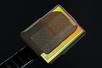
 HBM memory on an AMD Radeon R9 Nano graphics card's GPU package
.jpg)
.jpg)
.jpg)
Interface
The HBM DRAM is tightly coupled to the host compute die with a distributed interface. The interface is divided into independent channels. The channels are completely independent of one another and are not necessarily synchronous to each other. The HBM DRAM uses a wide-interface architecture to achieve high-speed, low-power operation. The HBM DRAM uses a 500 MHz differential clock CK_t / CK_c (where the suffix "_t" denotes the "true", or "positive", component of the differential pair, and "_c" stands for the "complementary" one). Commands are registered at the rising edge of CK_t, CK_c. Each channel interface maintains a 128‑bit data bus operating at double data rate (DDR). HBM supports transfer rates of 1 GT/s per pin (transferring 1 bit), yielding an overall package bandwidth of 128 GB/s.
HBM2
The second generation of High Bandwidth Memory, HBM2, also specifies up to eight dies per stack and doubles pin transfer rates up to 2 GT/s. Retaining 1024‑bit wide access, HBM2 is able to reach 256 GB/s memory bandwidth per package. The HBM2 spec allows up to 8 GB per package. HBM2 is predicted to be especially useful for performance-sensitive consumer applications such as virtual reality.
On January 19, 2016, Samsung announced early mass production of HBM2, at up to 8 GB per stack. SK Hynix also announced availability of 4 GB stacks in August 2016.
-
 HBM2 DRAM die
 -
 HBM2 controller die
 -
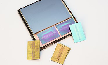 The HBM2 interposer of a Radeon RX Vega 64 GPU, with removed HBM dies; the GPU is still in place


HBM2E
In late 2018, JEDEC announced an update to the HBM2 specification, providing for increased bandwidth and capacities. Up to 307 GB/s per stack (2.5 Tbit/s effective data rate) is now supported in the official specification, though products operating at this speed had already been available. Additionally, the update added support for 12‑Hi stacks (12 dies) making capacities of up to 24 GB per stack possible.
On March 20, 2019, Samsung announced their Flashbolt HBM2E, featuring eight dies per stack, a transfer rate of 3.2 GT/s, providing a total of 16 GB and 410 GB/s per stack.
August 12, 2019, SK Hynix announced their HBM2E, featuring eight dies per stack, a transfer rate of 3.6 GT/s, providing a total of 16 GB and 460 GB/s per stack. On July 2, 2020, SK Hynix announced that mass production has begun.
HBM3
In late 2020, Micron unveiled that the HBM2E standard would be updated and alongside that they unveiled the next standard known as HBMnext (later renamed to HBM3). This was to be a big generational leap from HBM2 and the replacement to HBM2E. This new VRAM would have come to the market in the Q4 of 2022. This would likely introduce a new architecture as the naming suggests.
While the architecture might be overhauled, leaks point toward the performance to be similar to that of the updated HBM2E standard. This RAM is likely to be used mostly in data center GPUs.
In mid 2021, SK Hynix unveiled some specifications of the HBM3 standard, with 5.2 Gbit/s I/O speeds and bandwidth of 665 GB/s per package, as well as up to 16-high 2.5D and 3D solutions.
On 20 October 2021, before the JEDEC standard for HBM3 was finalised, SK Hynix was the first memory vendor to announce that it has finished development of HBM3 memory devices. According to SK Hynix, the memory would run as fast as 6.4 Gbps/pin, double the data rate of JEDEC-standard HBM2E, which formally tops out at 3.2 Gbps/pin, or 78% faster than SK Hynix’s own 3.6 Gbps/pin HBM2E. The devices support a data transfer rate of 6.4 Gbit/s and therefore a single HBM3 stack may provide a bandwidth of up to 819 GB/s. The basic bus widths for HBM3 remain unchanged, with a single stack of memory being 1024-bits wide. SK Hynix would offer their memory in two capacities: 16 GB and 24 GB, aligning with 8-Hi and 12-Hi stacks respectively. The stacks consist of 8 or 12 16 Gb DRAMs that are each 30 μm thick and interconnected using Through Silicon Vias (TSVs).
According to Ryan Smith of AnandTech, the SK Hynix first generation HBM3 memory has the same density as their latest-generation HBM2E memory, meaning that device vendors looking to increase their total memory capacities for their next-generation parts would need to use memory with 12 dies/layers, up from the 8 layer stacks they typically used until then. According to Anton Shilov of Tom's Hardware, high-performance compute GPUs or FPGAs typically use four or six HBM stacks, so with SK Hynix's HBM3 24 GB stacks they would accordingly get 3.2 TB/s or 4.9 TB/s of memory bandwidth. He also noted that SK Hynix's HBM3 chips are square, not rectangular like HBM2 and HBM2E chips. According to Chris Mellor of The Register, with JEDEC not yet having developed its HBM3 standard, might mean that SK Hynix would need to retrofit its design to a future and faster one.
JEDEC officially announced the HBM3 standard on January 27, 2022. The number of memory channels was doubled from 8 channels of 128 bits with HBM2e to 16 channels of 64 bits with HBM3. Therefore, the total number of data pins of the interface is still 1024.
In June 2022, SK Hynix announced they started mass production of industry's first HBM3 memory to be used with Nvidia's H100 GPU expected to ship in Q3 2022. The memory will provide H100 with "up to 819 GB/s" of memory bandwidth.
In August 2022, Nvidia announced that its "Hopper" H100 GPU will ship with five active HBM3 sites (out of six on board) offering 80 GB of RAM and 3 TB/s of memory bandwidth (16 GB and 600 GB/s per site).
HBM3E
On 30 May 2023, SK Hynix unveiled its HBM3E memory with 8 Gbps/pin data processing speed (25% faster than HBM3), which is to enter production in the first half of 2024. At 8 GT/s with 1024-bit bus, its bandwidth per stack is increased from 819.2 GB/s as in HBM3 to 1 TB/s.
On 26 July 2023, Micron announced its HBM3E memory with 9.2 Gbps/pin data processing speed (50% faster than HBM3). Micron HBM3E memory is a high-performance HBM that uses 1β DRAM process technology and advanced packaging to achieve the highest performance, capacity and power efficiency in the industry. It can store 24 GB per 8-high cube and allows data transfer at 1.2 TB/s. There will be a 12-high cube with 36 GB capacity in 2024.
In August 2023, Nvidia announced a new version of their GH200 Grace Hopper superchip that utilizes 141 GB (144 GiB physical) of HBM3e over a 6144-bit bus providing 50% higher memory bandwidth and 75% higher memory capacity over the HBM3 version.
In May 2023, Samsung announced HBM3P with up to 7.2 Gbps which will be in production in 2024.
On October 20 2023, Samsung announced their HBM3E "Shinebolt" with up to 9.8 Gbps memory.
On February 26 2024, Micron announced the mass production of Micron's HBM3E memory.
On March 18 2024, Nvidia announced the Blackwell series of GPUs using HBM3E memory
On March 19 2024, SK Hynix announced the mass production of SK Hynix's HBM3E memory.
HBM-PIM
In February 2021, Samsung announced the development of HBM with processing-in-memory (PIM). This new memory brings AI computing capabilities inside the memory, to increase the large-scale processing of data. A DRAM-optimised AI engine is placed inside each memory bank to enable parallel processing and minimise data movement. Samsung claims this will deliver twice the system performance and reduce energy consumption by more than 70%, while not requiring any hardware or software changes to the rest of the system.
History
Background
Die-stacked memory was initially commercialized in the flash memory industry. Toshiba introduced a NAND flash memory chip with eight stacked dies in April 2007, followed by Hynix Semiconductor introducing a NAND flash chip with 24 stacked dies in September 2007.
3D-stacked random-access memory (RAM) using through-silicon via (TSV) technology was commercialized by Elpida Memory, which developed the first 8 GB DRAM chip (stacked with four DDR3 SDRAM dies) in September 2009, and released it in June 2011. In 2011, SK Hynix introduced 16 GB DDR3 memory (40 nm class) using TSV technology, Samsung Electronics introduced 3D-stacked 32 GB DDR3 (30 nm class) based on TSV in September, and then Samsung and Micron Technology announced TSV-based Hybrid Memory Cube (HMC) technology in October.
JEDEC first released the JESD229 standard for Wide IO memory, the predecessor of HBM featuring four 128 bit channels with single data rate clocking, in December 2011 after several years of work. The first HBM standard JESD235 followed in October 2013.
Development

The development of High Bandwidth Memory began at AMD in 2008 to solve the problem of ever-increasing power usage and form factor of computer memory. Over the next several years, AMD developed procedures to solve die-stacking problems with a team led by Senior AMD Fellow Bryan Black. To help AMD realize their vision of HBM, they enlisted partners from the memory industry, particularly Korean company SK Hynix, which had prior experience with 3D-stacked memory, as well as partners from the interposer industry (Taiwanese company UMC) and packaging industry (Amkor Technology and ASE).
The development of HBM was completed in 2013, when SK Hynix built the first HBM memory chip. HBM was adopted as industry standard JESD235 by JEDEC in October 2013, following a proposal by AMD and SK Hynix in 2010. High volume manufacturing began at a Hynix facility in Icheon, South Korea, in 2015.
The first GPU utilizing HBM was the AMD Fiji which was released in June 2015 powering the AMD Radeon R9 Fury X.
In January 2016, Samsung Electronics began early mass production of HBM2. The same month, HBM2 was accepted by JEDEC as standard JESD235a. The first GPU chip utilizing HBM2 is the Nvidia Tesla P100 which was officially announced in April 2016.
In June 2016, Intel released a family of Xeon Phi processors with 8 stacks of HCDRAM, Micron's version of HBM. At Hot Chips in August 2016, both Samsung and Hynix announced a new generation HBM memory technologies. Both companies announced high performance products expected to have increased density, increased bandwidth, and lower power consumption. Samsung also announced a lower-cost version of HBM under development targeting mass markets. Removing the buffer die and decreasing the number of TSVs lowers cost, though at the expense of a decreased overall bandwidth (200 GB/s).
Nvidia announced Nvidia Hopper H100 GPU, the world's first GPU utilizing HBM3 on March 22, 2022.
See also
- Stacked DRAM
- eDRAM
- Chip stack multi-chip module
- Hybrid Memory Cube (HMC): stacked memory standard from Micron Technology (2011)
References
External links
- High Bandwidth Memory (HBM) DRAM (JESD235), JEDEC, October 2013
- Lee, Dong Uk; Kim, Kyung Whan; Kim, Kwan Weon; Kim, Hongjung; Kim, Ju Young; et al. (9–13 Feb 2014). "25.2 a 1.2V 8 Gb 8-channel 128 GB/S high-bandwidth memory (HBM) stacked DRAM with effective microbump I/O test methods using 29nm process and TSV". 2014 IEEE International Solid-State Circuits Conference Digest of Technical Papers (ISSCC). IEEE (published 6 March 2014). pp. 432–433. doi:10.1109/ISSCC.2014.6757501. ISBN 978-1-4799-0920-9. S2CID 40185587.
- HBM vs HBM2 vs GDDR5 vs GDDR5X Memory Comparison
This article uses material from the Wikipedia English article High Bandwidth Memory, which is released under the Creative Commons Attribution-ShareAlike 3.0 license ("CC BY-SA 3.0"); additional terms may apply (view authors). Content is available under CC BY-SA 4.0 unless otherwise noted. Images, videos and audio are available under their respective licenses.
®Wikipedia is a registered trademark of the Wiki Foundation, Inc. Wiki English (DUHOCTRUNGQUOC.VN) is an independent company and has no affiliation with Wiki Foundation.